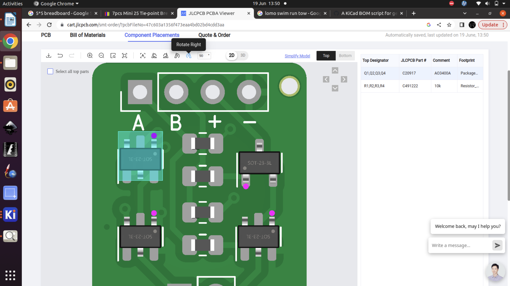
software crosschecking PCB component footprint and bom footprint.
Por um escritor misterioso
Descrição

EasyEDA Tutorial

EasyEDA Tutorial
KiCad: using a PCB assembly service — HackSpace magazine
Elementary, Mr. Watson: The Anatomy of Your Component—Footprint
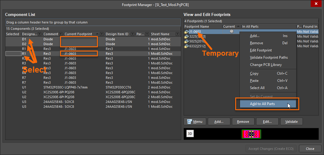
KB: Update schematic component with a new footprint

Getting BOM information(including MPN if provided) using KiCad's
The Four PCB Component Footprint Basics for Your Next Design

How to design a PCB when the components used in the design are not

What does a “footprint” mean in PCB design? - Quora

How to Choose the Correct Component Footprint : 3 Steps
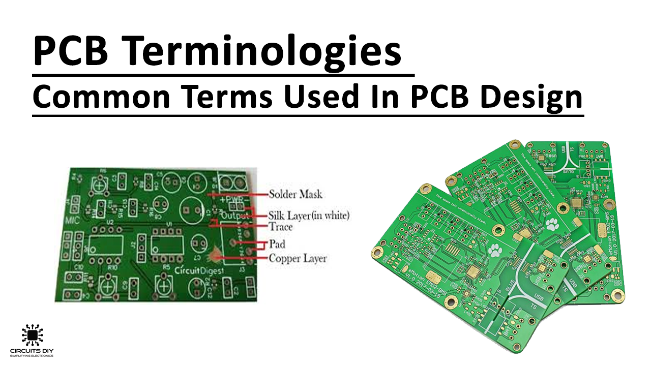
PCB Terminologies - Common Terms Used In PCB Design
de
por adulto (o preço varia de acordo com o tamanho do grupo)


format(webp))
